
Adapted by:
Juan Carlos López
Senior WriterAn engineer by training. A science and tech journalist by passion, vocation, and conviction. I've been writing professionally for over two decades, and I suspect I still have a long way to go. At Xataka, I write about many topics, but I mainly enjoy covering nuclear fusion, quantum physics, quantum computers, microprocessors, and TVs.

Karen Alfaro
WriterCommunications professional with a decade of experience as a copywriter, proofreader, and editor. As a travel and science journalist, I've collaborated with several print and digital outlets around the world. I'm passionate about culture, music, food, history, and innovative technologies.
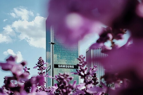
Samsung is slowly getting back on track. In mid-March, chairman Jay Y. Lee sent an internal statement summarizing the current situation: “Our technological edge has been compromised across all our businesses. It’s hard to see that efforts are being made to drive big innovation or tackle new challenges. There are only efforts to maintain a status quo rather than shaking things up.”
Samsung’s semiconductor manufacturing subsidiary is the engine of the company. To return to health, it must increase its competitiveness. However, to do that, its 2-nanometer (nm) integration technology must rival Intel’s and TSMC’s equivalent lithography nodes. Fortunately, Samsung starts from a favorable position. It has spent more than two years developing the most critical photolithography in its history.
Samsung Is Already Testing Its 2 nm Node for Nvidia and Qualcomm
At the beginning of January 2025, several reliable Asian media outlets reported that Samsung had begun testing 2 nm semiconductor production to secure initial customer agreements. At that time, Japanese AI chip designer Preferred Networks and a South Korean company specializing in neural processing units (NPUs) showed interest in having Samsung manufacture their designs on the new 2nm node.

Samsung must finalize several deals before competitors begin large-scale production with equivalent photolithography, especially during this delicate moment for the company. But that’s not all. Five months after that news broke, ChosunBiz, a South Korean media outlet known for its detailed semiconductor coverage, reported that Samsung had already started testing its 2 nm node for Nvidia and Qualcomm.
It’s reasonable to assume both Samsung and TSMC will manufacture 2 nm chips for these companies.
While testing doesn’t guarantee Samsung will manufacture 2 nm integrated circuits for the two U.S. companies, the interest in South Korean technology speaks volumes. If Samsung wins deals to produce Nvidia’s gaming and AI GPUs and Qualcomm’s SoCs, TSMC could lose critical ground.
It’s reasonable to assume both Samsung and TSMC will manufacture 2 nm chips for these companies. Additionally, Samsung plans to produce 2 nm semiconductors at its Texas fab, which could help it secure contracts with U.S. chip designers and avoid U.S. tariffs.
Image | Valentyn Chernetskyi (Unsplash)